

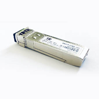
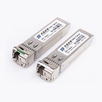
Features
l Hot pluggable QSFP28 MSA form factor
l Compliant to IEEE 802.3ba 100GBASE-LR4
l Up to 10km reach for G.652 SMF
l 1300nm LAN-WDM DFB-based Transmitter with optical MUX
l PIN Receiver ROSA with optical De-MUX
l 4x28G electrical serial interface (CEI-28G-VSR)
l Two wire serial interface with integrated digital monitor
l Duplex LC connector
l Single +3.3V power supply
l Maximum power consumption 4.5W
Operating case temperature: -5 ~ +70°C
Applications
l 100GBASE-LR4 Ethernet Links
l Infiniband QDR and DDR interconnects
l Client-side 100G Telecom connections
l Inter rack connections
Optical test system
Absolute Maximum Ratings
Parameter | Symbol | Min. | Typ. | Max. | Unit | Notes |
Power Supply Voltage | Vcc | 3.13 | 3.3 | 3.47 | V | |
Power Supply Current | Icc | - | - | 1300 | mA | |
Power Supply Current with Low Power Mode | Icc | - | - | 400 | mA | |
Case Operating Temperature | Top | -5 | - | 70 | °C | |
Data Rate | - | 103 | - | 112 | Gbps | |
Link Distance with G652 SMF | Lmax | - | - | 10 | Km | |
Baud Rate Tolerance | -100 | 100 | ppm |
Performance Specifications – Transmitter (-5C<Tc<+70°C; +2.97V<Vcc<+3.6V)
Parameter | Symbol | Min. | Typ. | Max. | Unit | Notes |
Input Differential Impedance | Zin | 90 | 100 | 110 | Ω | |
Input Amplitude (Differential) | Vin | - | - | 1050 | mV | |
Signaling Speed per Lane | BRavg | - | 25.78 | - | Gbps | |
Total Average Launch Optical Power | Pout | - | - | 10.5 | dBm | |
Average Launch Power per Lane | Peach | -4.3 | - | 4.5 | dBm | |
Extinction Ratio | ER | 4 | - | - | dB | |
Average Launch power of OFF TX each lane | Poff | - | - | -30 | dBm | |
Lane 0 Center Wavelength | λC0 | 1294.53 | 1295.56 | 1296.59 | nm | |
Lane 1 Center Wavelength | λC0 | 1299.02 | 1300.05 | 1301.09 | nm | |
Lane 2 Center Wavelength | λC0 | 1303.54 | 1304.58 | 1305.63 | nm | |
Lane 3 Center Wavelength | λC0 | 1308.09 | 1309.14 | 1310.19 | nm | |
Spectral Width(-20dB) | Δλ | - | - | 1 | nm | |
Side Mode Suppression Ratio | SMSR | 30 | - | - | dB | |
Relative Intensity Noise | RIN | - | - | -130 | dB/Hz | |
Optical Return Loss Tolerance | - | - | 20 | dB | ||
Transmitter and dispersion penalty (TDP), each lane (max) | DP | - | - | 2.2 | dB | |
Eye Diagram | IEEE802.3ba-2010 Compliant | |||||
Performance Specifications – Receiver (-5C<Tc<+70°C; +2.97V<Vcc<+3.6V)
Parameter | Symbol | Min. | Typ. | Max. | Unit | Notes |
Output Amplitude (Differential) | Vout | 200 | 1100 | mV | ||
Output Differential Impedance | Zin | 90 | 100 | 110 | Ω | |
Signaling Speed (per Lane) | BRavg | - | 25.78 | - | Gbps | |
Center Wavelength (per lane) | λ0 | 1294.53 | 1295.56 | 1596.59 | nm | |
λ1 | 1299.02 | 1300.05 | 1301.09 | nm | ||
λ2 | 1303.54 | 1304.58 | 1305.68 | nm | ||
λ3 | 1308.09 | 1309.14 | 1310.19 | nm | ||
Receiver Sensitivity (per lane) | PIN | - | - | -10.6 | dBm | |
Stressed Receiver Sensitivity in OMA (per lane) | - | - | - | -6.8 | dBm | 1 |
Receive power in OMA (per lane) | - | - | - | 4.5 | dBm | |
Damaged Threshold (per lane) | THd | 5.5 | - | - | dBm | 2 |
LOS Assert (per lane) | LOSA | -20 | - | - | dBm | |
LOS De-Assert (per lane) | LOSD | - | - | -15 | dBm | |
LOS Hysteresisi (per lane) | LOSH | 0.5 | - | - | dB | |
Receiver Reflectance | - | - | - | -26 | dB |
Note1: Measured with conformance test signal at receiver input for 1E-12 BER.
Note2: The receiver shall be able to tolerate, without damage, continuous exposure to a modulated optical input signal having this power level on per lane. The receiver does not have to operate correctly at this input power.
Digital Diagnostics Specifications
Parameter | Range | Accuracy | Unit | Calibration |
Power Voltage | 3.13~3.36 | ±0.1 | V | Internal |
Case Temperature | -5~+70 | ±3 | °C | Internal |
TX Bias Current(per Lane | 5~150 | ±10% | mA | Internal |
TX Optical Power(per lane) | -4.3~4.5 | ±3 | dB | Internal |
Rx Optical Power(per lane) | -10.6~+4.5 | ±3 | dB | Internal |
联系人:营销部
手机:0591-88000418
电话:0591-88000418
邮箱:support@brocess.com
地址: 福州高新区创新园二期18号楼
 kefu
kefu